FEI HELIOS NANOLAB 600I FIB/SEM
Location
CoorsTek 001-J
fei helios nanolab 6001 fib/sem POLICIES AND PROCEDURES
Billing schedule:
Charges are invoiced at the end of each calendar month. Internal charges are directly uploaded to Banner.
Supervisors should review charges in FOM each month to limit the need for manual adjustments after charges have been uploaded. Users may contact the facility director to discuss any disputed charges.
Rates are published on the website and calculated in consultation with the Controller’s office.
There is a minimum charge of 15 minutes of use.
Instrument Access:
FOM automatically disables scheduling access to this instrument for a user who has not used the instrument in over one year. A user who wishes to regain access should schedule a refresher training session with the instrument manager.
Reservations:
Reservations are made in half-hour time increments.
In order to promote additional usage while still providing less frequent users adequate access, daytime weekday reservations (8 AM – 5 PM) are limited in total hours per user per instrument at any given time. For the Helios this is set at 8 hours.
There is no limit on the number of hours reserved overnight and on weekends.
The schedule is open for reservation 14 days in advance. If special circumstances require reserving a time further in advance, contact the instrument manager.
A user can immediately access an unreserved instrument during the day (via express logon) regardless of other reservation limitations.
Daytime, Evening and Weekends:
In order to promote additional usage while still providing less frequent users adequate access, weekday daytime reservations (8 AM – 5 PM) are limited in total hours per user per instrument at any given time. For most instruments this is set at 8 hours.
There is no limit on the number of hours reserved overnight and on weekends.
There are currently no billing distinctions between day and evening use, however, in order to encourage the development of proficient users and not limit productive research, usage over 12 hours/month by one user on one project is charged at 30% of the hourly rate for this instrument.
Flexible start/end time:
Start/end time is calculated to the second so that you are billed for the actual instrument time you have used.
Unused reservation:
If user does not show up within 30 minutes after reserved start time, the reservation will be cancelled and another user may use the time period. The user who made the reservation will be charged a half hour no-show/late cancellation fee.
Cancelled reservation:
Late cancellations or no shows will be charged 50% of the reserved time. (If 2 hours were reserved, 1 hour of usage will be charged.)
Late cancellation is considered as cancellation fewer than 16 hours before the scheduled start time.
We will follow up individually with frequent offenders, with the possibility of temporarily suspending their scheduling access.
If there are extenuating circumstances, such as a medical emergency, the late cancellation fee will be waived.
If an instrument is down, users will not be charged for unused reservations and do not need to cancel their reservations.
Forgetting to login/logout:
Users should notify the instrument manager or leave a note in the FOM comments if they forgot to log in to FOM at the start of their session or forgot to log off FOM at the end of their session.
Report of equipment problem:
If an instrument is not functioning properly during the session, the user should notify the instrument manager as soon as possible. This can be done in person or in the comments in FOM. For reports in FOM, instrument managers will receive an email notice and address the problem as soon as possible. Instrument managers will also determine whether the usage charge should be reduced or waived due to the problem reported.
Specimen Prep Capabilities in the Electron Microscopy Lab
GENERAL
- Slow Speed Diamond Saws
- EVACTRON CombiClean Decontaminator
SEM
- JEOL IB-0910CP Cross-Section Polisher
- Hummer IV Sputtering System (Au Coater)
- Cressington Carbon Coater
TEM
- 3mm Foil Punch
- South Bay Model 350 3mm TEM Disk Cutter
- Gatan Model 600 Duo Mill Ar ion mill
- Fischione Electropolishing System
Instrument Details
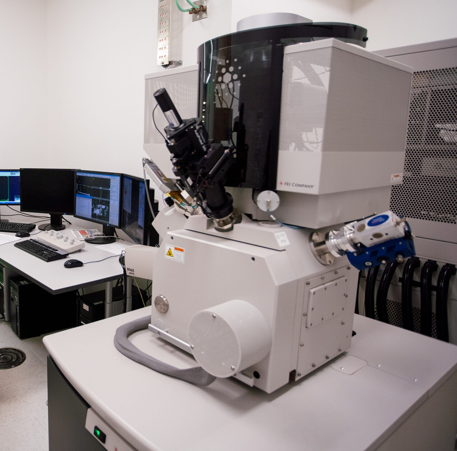
The Helios NanoLab 600i is a SEM/FIB DualBeam workstation with a Ga ion column for imaging and sample milling and Pt deposition (GIS) capability. Nanoscale chemical analysis may be performed with an EDAX energy dispersive X-ray spectroscopy (EDS) system. The instrument is also outfitted with an electron backscattered diffraction (EBSD) system, which allows for crystallographic determination on the nanoscale, and, along with imaging capabilities, 3-D reconstructions of the material composition and crystallography. In situ manipulation for TEM foil extraction is performed using an Omniprobe Autoprobe 200 nano-manipulator, with 10 nm positioning resolution.
- Schottky Field Emission Cathode
- Resolution: 0.9 nm at 15 kV (at eucentric WD); 1.4 nm at 1 kV (at optimum WD)
- Ga Source Focused Ion Beam (FIB) – 0.5 kV to 30 kV
- Platinum Deposition (GIS) System
- Secondary (SEI) and Backscatter (BEI) Imaging
- In-lens SE detector (TLD-SE)
- In-lens BSE detector (TLD-BSE)
- Everhardt-Thornley SE
- Solid-state BF and DF STEM detector
- AutoFIB, AutoTEM, Slice and View, and EBS3 Software
- EDAX “Octane Super” SDD Energy Dispersive Spectroscopy of X-rays (EDS)
- EDAX “Hikari Super” 1400pps Electron Backscatter Diffraction (EBSD) detector
- EDAX TEAM software
- Omniprobe Autoprobe™ 200 Nano-manipulator

Get Started or Request Training