LUCAS ENRIGHT
PhD Program, Materials Science
LUCAS ENRIGHT
PhD Program, Materials Science
 During my undergraduate studies at the University of Connecticut, I took a summer internship with the Air Force Research Lab at Kirtland AFB, New Mexico. My research with AFRL gave me hands-on experience with microwave measurements of materials and led me to pursue a PhD at Mines with microwave measurement research at NIST.
I am excited to be a part of the Quantum Engineering NSF Research Traineeship because it allows me to explore the fundamentals of quantum engineering without losing sight of the science and engineering that originally brought me here. I am excited to work more closely with the world of quantum engineering and collaborate with diverse groups throughout academia, national labs, and industry.
In my free time I enjoy reading, hiking, and exploring local breweries. I do miss New England fall, but I do not miss New England winter.
Education
BS, Materials Science and Engineering, University of Connecticut
Research Interests
- Low-loss dielectrics
- Microwave measurements of materials
Current Project
Standard reference material for dielectric properties
With the development and rollout of 5G millimeter-wave (mmWave) technology, manufacturers need standards to validate measurements techniques, accept new materials, and for quality assurance. Traceability in low-loss microwave measurements will have important implications in telecommunications and in quantum information.
This project incorporates heavy collaboration with industry for measurement validation and feedback on the design of the standards.
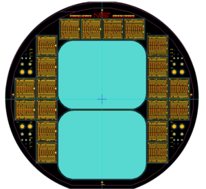
A 4” wafer layout that allows us to laser dice the wafer into components for resonant cavity (blue coupons) and on-wafer (gold transmission lines) measurements of permittivity. The on-wafer measurements are a way to validate the results we get from our resonant cavity measurements and a way to interpolate between the resonance frequencies of those cavities.
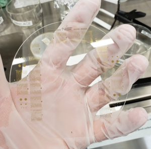
A prototype standard made from a 4” high-purity fused silica wafer with the layout shown in “Picture1” after photolithography. This wafer still needs to be diced before we can make measurements in a resonant cavity or on-wafer.
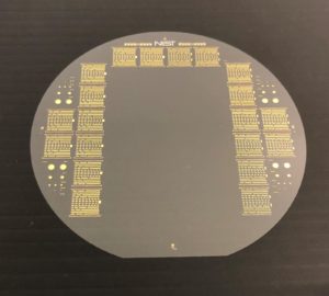
Same as above, just a different angle. A little blurry, but at least my hand isn’t taking up most of the photo.
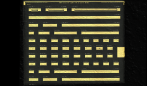
A laser microscope image of one of the on-wafer measurement kits after laser dicing. With these kits, we can use multiline TRL (thru-reflect-line) to extract the material properties of our substrate across a broad frequency range (0.1 GHz – 300 GHz).
Mentors
- Nate Orloff, NIST
- Geoff Brennecka, Metallurgical and Materials Engineering
